
終於倒數第三天啦!! 不過今天還是要來繼續奮戰一下!!
今天呢! 要來介紹一個我覺得蠻有趣的Flash燒錄方式:"Target Burner"名子是我亂取的
這個實作的方式,主要是我在研究「GitHub: riscv/riscv-openocd」時候,所看到一個蠻有趣的應用!
內容接續上篇「Day 27: 高手不輕易透露的技巧 - Flash Programming」,講述Sifive在"GitHub: riscv/riscv-openocd"中實作的"fespi" Flash Driver,以及裡面write flash中所使用到的"Target Burner"背後的原理和實作細節!
對了,再提醒一下!
我沒有要廣告任何Sifive相關的東西的意思
謝謝!
在開始剖析fespi的內容之前,我們先來看看"N25Q128"的Commmand Table!
請參考「N25Q128 with Subsector Erase on Boot Sectors」的內容!
這邊節錄一些待會會用到的指令:
再過來介紹Status Register的內容:
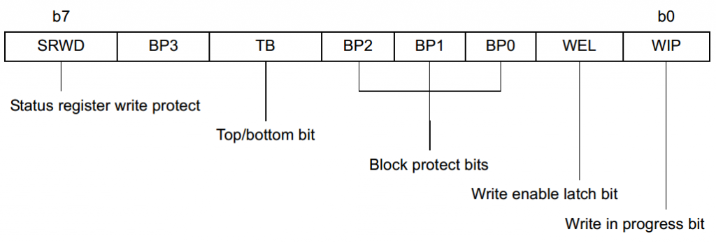
--引用自N25Q128 with Subsector Erase on Boot Sectors
目前只會使用到其中的兩個bits,基本定義如下:
剩下的內容就留給有興趣的讀者去研究吧,大概183頁而已!!!!!
再來介紹一下,E300中所使用到的SPI Controller!
還記的這篇Lab嗎!? 「Day 22: [Lab] 深入淺出 RISC-V 源碼剖析 (Final) - 執行 & Log分析」,在這邊,我們使用Xilinx Arty開發版,配合SiFive E51 FPGA Eval Kit v1p0突然發現那篇忘了放連結XDD
裡面有包含一個SPI Controller,因為待會fespi Flash Driver都會跟他有關,因此在這邊簡單介紹一下,常用到的Registers!
有錯請在留言處提出,他們的IP我也不太熟*
先來看看Registers Table:
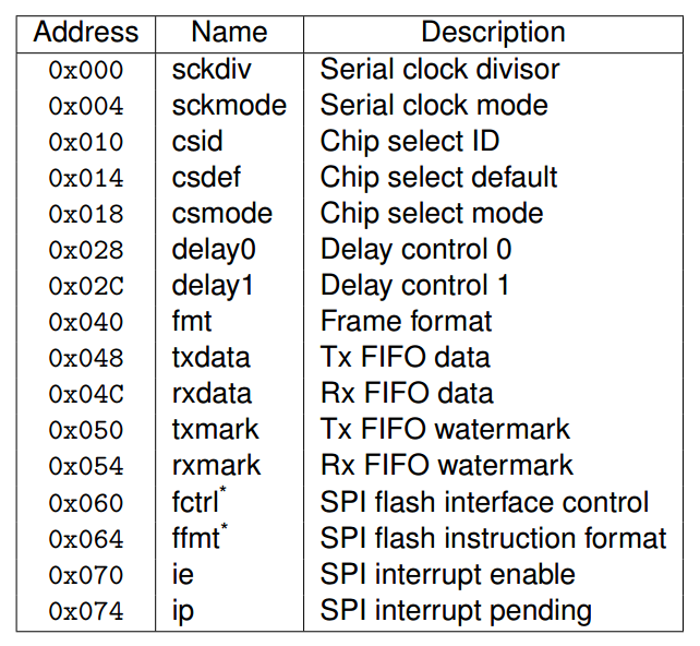
--引用自Freedom E300 Platform Reference Manual
底下介紹幾個有用到的Register!
--引用自Freedom E300 Platform Reference Manual
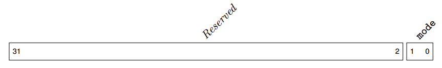
主要是讓SPI Controller可以選擇正確的Flash,拉起對應的CS pin,
包含以下幾種Mode:
--引用自Freedom E300 Platform Reference Manual
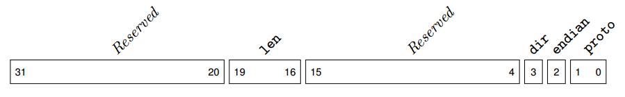
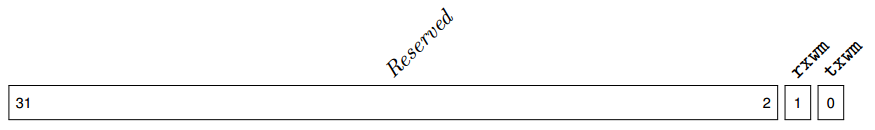
這個Register主要控制FIFO傳輸的方式,定義如下:
--引用自Freedom E300 Platform Reference Manual
--引用自Freedom E300 Platform Reference Manual
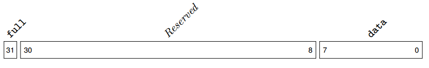
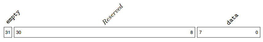
這兩個比較類似,放在一起!
主要是傳輸/接收的資料的FIFO,裡面還包含指示目前狀態的Flag:
另外提醒一下,實作中所使用的名稱,與文件上不相同,
對照的時候需要注意一下(src/flash/nor/fespi.c)::
#define FESPI_REG_TXFIFO          0x48
#define FESPI_REG_RXFIFO          0x4c
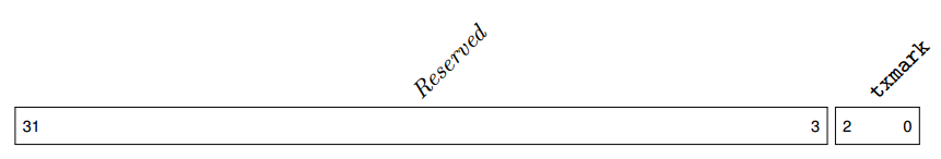
--引用自Freedom E300 Platform Reference Manual
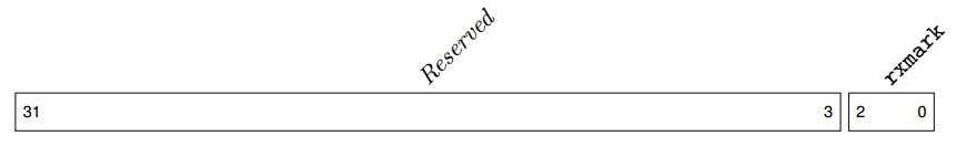
--引用自Freedom E300 Platform Reference Manual
當Tx的剩餘FIFO內容小於$txmark所設定的時候,自動將Interrupt拉起!
至於$rxmark在實作中沒有用到,放在這邊給大家參考一下而已XD!
另外提醒一下,實作中所使用的名稱,與文件上不相同,
對照的時候需要注意一下(src/flash/nor/fespi.c)::
#define FESPI_REG_TXCTRL          0x50
#define FESPI_REG_RXCTRL          0x54
--引用自Freedom E300 Platform Reference Manual
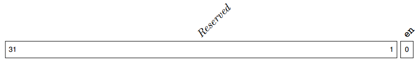
在Sifive的設計當中,主要分成兩種操作模式:
--引用自Freedom E300 Platform Reference Manual
這邊主要是控制Interrupt的Enabled和指示目前狀態!
當Tx的剩餘FIFO內容小於$txmark所設定的時候,如果$ie中的txwm有Enabled的話,
則$ip的txwm會被自動拉起來,表示目前Tx FIFO已空!
同理Rx也是類似的概念!
以上終於 報告 介紹完畢,開始正式進入今天的主題內容--
fespi(Freedom E SPI controller) Flash Driver
上篇有提到,每個Bank都需要搭配自己的一套Flash Driver,幾本上Flash Driver應該包含的內容,如下所示,請參考(src/flash/nor/driver.h):
struct flash_driver {
    const char *name;
    const char *usage;
    const struct command_registration *commands;
    __FLASH_BANK_COMMAND((*flash_bank_command));
    int (*erase)(struct flash_bank *bank, int first, int last);
    int (*protect)(struct flash_bank *bank, int set, int first, int last);
    int (*write)(struct flash_bank *bank,
            const uint8_t *buffer, uint32_t offset, uint32_t count);
    int (*read)(struct flash_bank *bank,
            uint8_t *buffer, uint32_t offset, uint32_t count);
    int (*probe)(struct flash_bank *bank);
    int (*erase_check)(struct flash_bank *bank);
    int (*protect_check)(struct flash_bank *bank);
    int (*info)(struct flash_bank *bank, char *buf, int buf_size);
    int (*auto_probe)(struct flash_bank *bank);
};
詳細內容如下:
底下的章節中,將會剖析fespi在其中幾個比較重要的函式的實作內容!
至於沒說明的部分,剩下留給讀者自行研究啦!!
如果讀者有仔細觀察過「Day 22: [Lab] 深入淺出 RISC-V 源碼剖析 (Final) - 執行 & Log分析」這篇所使用的Config,就不難發下裡面偷偷的使用到了一項設定:
flash bank spi0 fespi 0x40000000 0 0 0 $_TARGETNAME 0x20004000 #譯註: 定義Flash區塊
這個Config就會讓OpenOCD定義一個全新的Bank,叫做"spi0",然後必須使用"fespi"這套Flash Driver!
讓我們看一下fespi_flash_bank_command()中的實作,
請參考(src/flash/nor/fespi.c):
FLASH_BANK_COMMAND_HANDLER(fespi_flash_bank_command)
{
    struct fespi_flash_bank *fespi_info;

    LOG_DEBUG("%s", __func__);

    if (CMD_ARGC < 6)
        return ERROR_COMMAND_SYNTAX_ERROR;

    fespi_info = malloc(sizeof(struct fespi_flash_bank));   ///譯註: 建立內部資料結構
    if (fespi_info == NULL) {
        LOG_ERROR("not enough memory");
        return ERROR_FAIL;
    }

    bank->driver_priv = fespi_info;
    fespi_info->probed = 0;
    fespi_info->ctrl_base = 0;

    ///譯註: 如果Config中有接上專用的參數
    if (CMD_ARGC >= 7) {
        int temp;
        COMMAND_PARSE_NUMBER(int, CMD_ARGV[6], temp);
        fespi_info->ctrl_base = (uint32_t) temp;
        LOG_DEBUG("ASSUMING FESPI device at ctrl_base = 0x%x", fespi_info->ctrl_base);
    }

    return ERROR_OK;
}
從這邊不難發現,Config最後面所接的"0x20004000",其實就是SPI Contorller的位置!
在這邊,簡單的準備好內部資料結構,然後把Controller的Base給存放起來!
這兩個處理過程比較類似! 應該說是幾本上一樣XD
主要負責初始化這個Bank中內部的Setors資料內容!
先來看一下fespi_auto_probe()的內容,請參考(src/flash/nor/fespi.c):
static int fespi_auto_probe(struct flash_bank *bank)
{
    struct fespi_flash_bank *fespi_info = bank->driver_priv;
    if (fespi_info->probed)
        return ERROR_OK;
    return fespi_probe(bank);
}
沒錯,就是直接呼叫fespi_probe()來做初始化,
不過要記得! 初始化只需要一次即可!
來看看fespi_probe()的內容吧,請參考(src/flash/nor/fespi.c):
static int fespi_probe(struct flash_bank *bank)
{
    struct target *target = bank->target;
    struct fespi_flash_bank *fespi_info = bank->driver_priv;
    uint32_t ctrl_base;
    struct flash_sector *sectors;
    uint32_t id = 0; /* silence uninitialized warning */
    const struct fespi_target *target_device;
    int retval;

    if (fespi_info->probed)
        free(bank->sectors);
    fespi_info->probed = 0;

    ///譯註 Step 1: 尋找SPI Controller Base
    if (fespi_info->ctrl_base == 0) {
        for (target_device = target_devices ; target_device->name ; ++target_device)
            if (target_device->tap_idcode == target->tap->idcode)
                break;

        if (!target_device->name) {
            LOG_ERROR("Device ID 0x%" PRIx32 " is not known as FESPI capable",
                    target->tap->idcode);
            return ERROR_FAIL;
        }

        fespi_info->ctrl_base = target_device->ctrl_base;

        LOG_DEBUG("Valid FESPI on device %s at address 0x%" PRIx32,
                target_device->name, bank->base);

    } else {
      LOG_DEBUG("Assuming FESPI as specified at address 0x%x with ctrl at 0x%x",
            fespi_info->ctrl_base,
            bank->base);
    }
    ctrl_base = fespi_info->ctrl_base;

    ///譯註 Step 2: 尋找Flash ID
    /* read and decode flash ID; returns in SW mode */
    FESPI_WRITE_REG(FESPI_REG_TXCTRL, FESPI_TXWM(1));
    fespi_set_dir(bank, FESPI_DIR_TX);

    retval = fespi_read_flash_id(bank, &id);

    FESPI_ENABLE_HW_MODE();
    if (retval != ERROR_OK)
        return retval;

    fespi_info->dev = NULL;
    for (const struct flash_device *p = flash_devices; p->name ; p++)
        if (p->device_id == id) {
            fespi_info->dev = p;
            break;
        }

    if (!fespi_info->dev) {
        LOG_ERROR("Unknown flash device (ID 0x%08" PRIx32 ")", id);
        return ERROR_FAIL;
    }

    LOG_INFO("Found flash device \'%s\' (ID 0x%08" PRIx32 ")",
            fespi_info->dev->name, fespi_info->dev->device_id);

    /* Set correct size value */
    bank->size = fespi_info->dev->size_in_bytes;

    ///譯註 Step 3: 初始化Sectors
    /* create and fill sectors array */
    bank->num_sectors =
        fespi_info->dev->size_in_bytes / fespi_info->dev->sectorsize;
    sectors = malloc(sizeof(struct flash_sector) * bank->num_sectors);
    if (sectors == NULL) {
        LOG_ERROR("not enough memory");
        return ERROR_FAIL;
    }

    for (int sector = 0; sector < bank->num_sectors; sector++) {
        sectors[sector].offset = sector * fespi_info->dev->sectorsize;
        sectors[sector].size = fespi_info->dev->sectorsize;
        sectors[sector].is_erased = -1;
        sectors[sector].is_protected = 1;
    }

    bank->sectors = sectors;
    fespi_info->probed = 1;
    return ERROR_OK;
}
看起來複雜,讓我們一一來剖析他!
首先是Step 1,尋找SPI Controller Base,這邊不難發現,如果剛剛Config已經指定的話(以上述例子: 0x20004000),那這邊就會跳過,反之,如果沒有指定的話,這邊採用idcode轉Controller Base的方式,請參考(src/flash/nor/fespi.c):
static const struct fespi_target target_devices[] = {
    /* name,   tap_idcode, ctrl_base */
    { "Freedom E300 SPI Flash",  0x10e31913 , 0x10014000 },
    { NULL,    0,           0          }
};
不過他只支援一種對應方式XDD
再來是Step 2,尋找Flash ID!
終於進入我們第一筆SPI Tx/Rx的流程當中!
首先先設定$txmark(忘記的話往上捲),請參考(src/flash/nor/fespi.c):
#define FESPI_WRITE_REG(a, v)                   \
{                               \
    int __r;                        \
                                \
    __r = target_write_u32(target, ctrl_base + (a), (v));   \
    if (__r != ERROR_OK) {                  \
        LOG_ERROR("FESPI_WRITE_REG error");     \
        return __r;                 \
    }                           \
}

FESPI_WRITE_REG(FESPI_REG_TXCTRL, FESPI_TXWM(1));
這邊其實就是呼叫OpenOC的target_write_u32(),然後對應的位置就是SPI Controller的Base再加上0x50($txmark的Address),然後把對應的值(這邊是0x1)寫入!
然後是fespi_set_dir(bank, FESPI_DIR_TX);,請參考(src/flash/nor/fespi.c):
static int fespi_set_dir(struct flash_bank *bank, bool dir)
{
    struct target *target = bank->target;
    struct fespi_flash_bank *fespi_info = bank->driver_priv;
    uint32_t ctrl_base = fespi_info->ctrl_base;

    FESPI_WRITE_REG(FESPI_REG_FMT,
            (FESPI_READ_REG(FESPI_REG_FMT) & ~(FESPI_FMT_DIR(0xFFFFFFFF))) |
            FESPI_FMT_DIR(dir));

    return ERROR_OK;

}
一樣是呼叫FESPI_WRITE_REG,然後去設定$fmt中的dir為Tx!
最後呼叫fespi_read_flash_id()來讀取ID,請參考(src/flash/nor/fespi.c):
static int fespi_read_flash_id(struct flash_bank *bank, uint32_t *id)
{
    struct target *target = bank->target;
    struct fespi_flash_bank *fespi_info = bank->driver_priv;
    uint32_t ctrl_base = fespi_info->ctrl_base;
    int retval;

    if (target->state != TARGET_HALTED) {
        LOG_ERROR("Target not halted");
        return ERROR_TARGET_NOT_HALTED;
    }

    fespi_txwm_wait(bank);

    /* Disable Hardware accesses*/
    FESPI_DISABLE_HW_MODE();

    /* poll WIP */
    retval = fespi_wip(bank, FESPI_PROBE_TIMEOUT);
    if (retval != ERROR_OK)
        return retval;

    fespi_set_dir(bank, FESPI_DIR_RX);

    /* Send SPI command "read ID" */
    FESPI_WRITE_REG(FESPI_REG_CSMODE, FESPI_CSMODE_HOLD);

    fespi_tx(bank, SPIFLASH_READ_ID);
    /* Send dummy bytes to actually read the ID.*/
    fespi_tx(bank, 0);
    fespi_tx(bank, 0);
    fespi_tx(bank, 0);

    /* read ID from Receive Register */
    *id = 0;
    if (fespi_rx(bank, NULL) != ERROR_OK)
        return ERROR_FAIL;
    uint8_t rx;
    if (fespi_rx(bank, &rx) != ERROR_OK)
        return ERROR_FAIL;
    *id = rx;
    if (fespi_rx(bank, &rx) != ERROR_OK)
        return ERROR_FAIL;
    *id |= (rx << 8);
    if (fespi_rx(bank, &rx) != ERROR_OK)
        return ERROR_FAIL;
    *id |= (rx << 16);

    FESPI_WRITE_REG(FESPI_REG_CSMODE, FESPI_CSMODE_AUTO);

    fespi_set_dir(bank, FESPI_DIR_TX);

    return ERROR_OK;
}
這邊的流程可以簡化如下:
讓我們看看實際執行的成果:
Info : 6533 4570 fespi.c:1094 fespi_probe(): Found flash device 'micron n25q128' (ID 0x0018ba20)
OK! 看起來正確,跟文件「N25Q128 with Subsector Erase on Boot Sectors」的內容相同!
最後回到fespi_probe()的Step 3,初始化Sectors!
    /* create and fill sectors array */
    bank->num_sectors =
        fespi_info->dev->size_in_bytes / fespi_info->dev->sectorsize;
    sectors = malloc(sizeof(struct flash_sector) * bank->num_sectors);
    if (sectors == NULL) {
        LOG_ERROR("not enough memory");
        return ERROR_FAIL;
    }

    for (int sector = 0; sector < bank->num_sectors; sector++) {
        sectors[sector].offset = sector * fespi_info->dev->sectorsize;
        sectors[sector].size = fespi_info->dev->sectorsize;
        sectors[sector].is_erased = -1;
        sectors[sector].is_protected = 1;
    }

    bank->sectors = sectors;
    fespi_info->probed = 1;
這個Flash中的Sector固定為64KB,因此可以用簡單的for loop計算出每個Sector的offset,然後順便設定size、is_erase(設定成Unknown)和is_protected(設定成Protected/Locked)!
最後已經初始化完畢的話,記得把probed設成1:
fespi_info->probed = 1;
搞定! 收工!
有了前面fespi_read_flash_id()的剖析後,讓我們來研究如何將Flash進行Erase,
請參考(src/flash/nor/fespi.c):
static int fespi_erase(struct flash_bank *bank, int first, int last)
{
    ....前面判斷 & 初始化省略XD

    for (sector = first; sector <= last; sector++) {
        retval = fespi_erase_sector(bank, sector);
        if (retval != ERROR_OK)
            break;
        keep_alive();
    }

    ....後面不重要
}
為了省篇幅,我們直接看到最重要的部分!
簡單的來說,就是針對一個個Sector去呼叫fespi_erase_sector()來清除該Sector!
所以直接看fespi_erase_sector()的內容,請參考(src/flash/nor/fespi.c):
static int fespi_erase_sector(struct flash_bank *bank, int sector)
{
    struct target *target = bank->target;
    struct fespi_flash_bank *fespi_info = bank->driver_priv;
    uint32_t ctrl_base = fespi_info->ctrl_base;
    int retval;

    retval = fespi_tx(bank, SPIFLASH_WRITE_ENABLE);
    if (retval != ERROR_OK)
        return retval;
    retval = fespi_txwm_wait(bank);
    if (retval != ERROR_OK)
        return retval;

    FESPI_WRITE_REG(FESPI_REG_CSMODE, FESPI_CSMODE_HOLD);
    retval = fespi_tx(bank, fespi_info->dev->erase_cmd);
    if (retval != ERROR_OK)
        return retval;
    sector = bank->sectors[sector].offset;
    retval = fespi_tx(bank, sector >> 16);
    if (retval != ERROR_OK)
        return retval;
    retval = fespi_tx(bank, sector >> 8);
    if (retval != ERROR_OK)
        return retval;
    retval = fespi_tx(bank, sector);
    if (retval != ERROR_OK)
        return retval;
    retval = fespi_txwm_wait(bank);
    if (retval != ERROR_OK)
        return retval;
    FESPI_WRITE_REG(FESPI_REG_CSMODE, FESPI_CSMODE_AUTO);

    retval = fespi_wip(bank, FESPI_MAX_TIMEOUT);
    if (retval != ERROR_OK)
        return retval;

    return ERROR_OK;
}
好,太複雜了,簡化如下:
以上就是Erase的內容,非常簡單吧!!
嘿嘿嘿!! 終於到今天的重頭戲啦!!!
既然講到Flash燒綠,怎可能不提到Write(Program)的實作!
當初在實驗這個Sifive提供的這個Target時,就意外發現他的燒綠速度非比尋常!
在剖析整套程式碼後,才發現這個有趣的設計,就讓我們來看看後面隱藏的秘密以及相關實作的內容吧!
仔細觀察一下剛剛所提到的"Read ID"和"Erase Sector"的流程,
不難發現它類似下面這張圖:
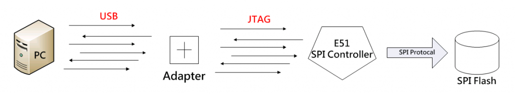
你會發現,每做一次的Tx/Rx就是一道、一道的USB + JTAG + SPI傳輸,
尤其是PC到Adapter的USB傳輸,中間的速度非常的慢!
換個角度想,如果沒辦法避免大量的USB+JTAG+SPI傳輸,
Burner本身的速度就會非常的緩慢,慢到使用者不能接受!
那如果假設今天有一個方法,可以一次搬移一堆資料到Target端,由Target端負責SPI Controller的處理,讓他慢慢讀寫完SPI Flash後,再回報成果!
我們是不是就能夠加速這個處理流程,例如下圖的方式:
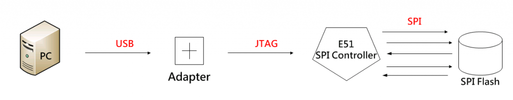
先一次將資料搬到Target上的RAM/ILM/DLM/....等可以讀、寫、執行指令的地方,
然後透過一個預先設計好放在上面的"小程式",負責將一筆筆的資料透過SPI Controller寫入到SPI Flash上,是不是就能加速啊!!
這個流程,就稱為"Target Burner"?! 我承認是自己亂命名的XD
以上就是整個背後的原理,接下來剖析如何實現這個功能!
那既然上面提到這個預先設計好放在上面的"小程式",
就要來剖析一下他擁有的功能啦!!
我們先來看看內容:
static const uint8_t algorithm_bin[] = {
     0x6f, 0x00, 0xc0, 0x01, 0x73, 0x00, 0x10, 0x00, 0x6f, 0x00, 0xc0, 0x02,
     0x6f, 0x00, 0x00, 0x05, 0x6f, 0x00, 0xc0, 0x05, 0x6f, 0x00, 0x00, 0x07,
     0x6f, 0x00, 0x00, 0x0a, 0x83, 0xc2, 0x05, 0x00, 0x93, 0x85, 0x15, 0x00,
     0x17, 0x03, 0x00, 0x00, 0x13, 0x03, 0xc3, 0xfd, 0xb3, 0x82, 0x62, 0x00,
     0x67, 0x80, 0x02, 0x00, 0x03, 0xc3, 0x05, 0x00, 0x93, 0x85, 0x15, 0x00,
     0x83, 0x22, 0x85, 0x04, 0xe3, 0xce, 0x02, 0xfe, 0x83, 0xc2, 0x05, 0x00,
     0x23, 0x24, 0x55, 0x04, 0x93, 0x85, 0x15, 0x00, 0x13, 0x03, 0xf3, 0xff,
     0xe3, 0x44, 0x60, 0xfe, 0x6f, 0xf0, 0x5f, 0xfc, 0x83, 0x22, 0x45, 0x07,
     0x93, 0xf2, 0x12, 0x00, 0xe3, 0x8c, 0x02, 0xfe, 0x6f, 0xf0, 0x5f, 0xfb,
     0x83, 0xc2, 0x05, 0x00, 0xb3, 0x82, 0xa2, 0x00, 0x03, 0xc3, 0x15, 0x00,
     0x93, 0x85, 0x25, 0x00, 0x23, 0xa0, 0x62, 0x00, 0x6f, 0xf0, 0xdf, 0xf9,
     0x13, 0x06, 0x50, 0x00, 0xef, 0x00, 0x80, 0x01, 0x13, 0x06, 0x00, 0x00,
     0xef, 0x00, 0x00, 0x01, 0x93, 0x72, 0x16, 0x00, 0xe3, 0x9a, 0x02, 0xfe,
     0x6f, 0xf0, 0x1f, 0xf8, 0x83, 0x22, 0x85, 0x04, 0xe3, 0xce, 0x02, 0xfe,
     0x23, 0x24, 0xc5, 0x04, 0x03, 0x26, 0xc5, 0x04, 0xe3, 0x4e, 0x06, 0xfe,
     0x67, 0x80, 0x00, 0x00, 0x83, 0x22, 0x05, 0x04, 0x13, 0x03, 0x70, 0xff,
     0xb3, 0xf2, 0x62, 0x00, 0x03, 0xc3, 0x05, 0x00, 0x93, 0x85, 0x15, 0x00,
     0xb3, 0xe2, 0x62, 0x00, 0x23, 0x20, 0x55, 0x04, 0x6f, 0xf0, 0x9f, 0xf4
};
好,結束!
開玩笑地,這個內容沒啥人可以直接看懂XD!
換成以下方式,請參考(src/flash/nor/fespi.c):
        .global _start
_start:
command_table:
        j       main            // 0
        ebreak                  // 4
        j       tx              // 8
        j       txwm_wait       // 12
        j       write_reg       // 16
        j       wip_wait        // 20
        j       set_dir         // 24

// Execute the program.
main:
        lbu     t0, 0(a1)
        addi    a1, a1, 1
        la      t1, command_table
        add     t0, t0, t1
        jr      t0

// Read 1 byte the contains the number of bytes to transmit. Then read those
// bytes from the program and transmit them one by one.
tx:
        lbu     t1, 0(a1)       // read number of bytes to transmit
        addi    a1, a1, 1
1:      lw      t0, FESPI_REG_TXFIFO(a0)        // wait for FIFO clear
        bltz    t0, 1b
        lbu     t0, 0(a1)       // Load byte to write
        sw      t0, FESPI_REG_TXFIFO(a0)
        addi    a1, a1, 1
        addi    t1, t1, -1
        bgtz    t1, 1b
        j       main

// Wait until TXWM is set.
txwm_wait:
1:      lw      t0, FESPI_REG_IP(a0)
        andi    t0, t0, FESPI_IP_TXWM
        beqz    t0, 1b
        j       main

// Read 1 byte that contains the offset of the register to write, and 1 byte
// that contains the data to write.
write_reg:
        lbu     t0, 0(a1)       // read register to write
        add     t0, t0, a0
        lbu     t1, 1(a1)       // read value to write
        addi    a1, a1, 2
        sw      t1, 0(t0)
        j       main

wip_wait:
        li      a2, SPIFLASH_READ_STATUS
        jal     txrx_byte
        // discard first result
1:      li      a2, 0
        jal     txrx_byte
        andi    t0, a2, SPIFLASH_BSY_BIT
        bnez    t0, 1b
        j       main

txrx_byte:  // transmit the byte in a2, receive a bit into a2
        lw      t0, FESPI_REG_TXFIFO(a0)        // wait for FIFO clear
        bltz    t0, txrx_byte
        sw      a2, FESPI_REG_TXFIFO(a0)
1:      lw      a2, FESPI_REG_RXFIFO(a0)
        bltz    a2, 1b
        ret

set_dir:
        lw      t0, FESPI_REG_FMT(a0)
        li      t1, ~(FESPI_FMT_DIR(0xFFFFFFFF))
        and     t0, t0, t1
        lbu     t1, 0(a1)       // read value to OR in
        addi    a1, a1, 1
        or      t0, t0, t1
        sw      t0, FESPI_REG_FMT(a0)
        j       main
有沒有比較好懂一點,基本上他提供以下7種功能,分別用進入點的位置(command_table)表示:
可以把這個小程式當作是一個小小小的"Assembler"!
只要我們負責把對應的指令&資料設定好,寫入Target上某塊空間後,再呼叫這個小程式來執行對應的內容,和寫入對應的資料!
這邊給個小提示:
$a0 裡面的內容是SPI Controller的Base Address
$a1 裡面的內容是指向這個指令&資料目前執行到的位置
基本內容如下,請參考(src/flash/nor/fespi.c):
static int fespi_write(struct flash_bank *bank, const uint8_t *buffer,
        uint32_t offset, uint32_t count)
{
    struct target *target = bank->target;
    struct fespi_flash_bank *fespi_info = bank->driver_priv;
    uint32_t ctrl_base = fespi_info->ctrl_base;
    uint32_t cur_count, page_size, page_offset;
    int sector;
    int retval = ERROR_OK;

    LOG_DEBUG("%s: offset=0x%08" PRIx32 " count=0x%08" PRIx32,
            __func__, offset, count);

    if (target->state != TARGET_HALTED) {
        LOG_ERROR("Target not halted");
        return ERROR_TARGET_NOT_HALTED;
    }

    if (offset + count > fespi_info->dev->size_in_bytes) {
        LOG_WARNING("Write past end of flash. Extra data discarded.");
        count = fespi_info->dev->size_in_bytes - offset;
    }

    /* Check sector protection */
    for (sector = 0; sector < bank->num_sectors; sector++) {
        /* Start offset in or before this sector? */
        /* End offset in or behind this sector? */
        if ((offset <
                    (bank->sectors[sector].offset + bank->sectors[sector].size))
                && ((offset + count - 1) >= bank->sectors[sector].offset)
                && bank->sectors[sector].is_protected) {
            LOG_ERROR("Flash sector %d protected", sector);
            return ERROR_FAIL;
        }
    }

    struct working_area *algorithm_wa;
    if (target_alloc_working_area(target, sizeof(algorithm_bin),
                &algorithm_wa) != ERROR_OK) {
        LOG_WARNING("Couldn't allocate %zd-byte working area.",
                sizeof(algorithm_bin));
        algorithm_wa = NULL;
    } else {
        retval = target_write_buffer(target, algorithm_wa->address,
                sizeof(algorithm_bin), algorithm_bin);
        if (retval != ERROR_OK) {
            LOG_ERROR("Failed to write code to 0x%" TARGET_PRIxADDR ": %d",
                    algorithm_wa->address, retval);
            target_free_working_area(target, algorithm_wa);
            algorithm_wa = NULL;
        }
    }

    struct working_area *data_wa = NULL;
    unsigned data_wa_size = 2 * count;
    while (1) {
        if (data_wa_size < 128) {
            LOG_WARNING("Couldn't allocate data working area.");
            target_free_working_area(target, algorithm_wa);
            algorithm_wa = NULL;
        }
        if (target_alloc_working_area_try(target, data_wa_size, &data_wa) ==
                ERROR_OK) {
            break;
        }

        data_wa_size /= 2;
    }

    page_size = fespi_info->dev->pagesize;

    fespi_txwm_wait(bank);

    /* Disable Hardware accesses*/
    FESPI_DISABLE_HW_MODE();

    /* poll WIP */
    retval = fespi_wip(bank, FESPI_PROBE_TIMEOUT);
    if (retval != ERROR_OK)
        return retval;

    struct algorithm_steps *as = as_new(count / 4);

    /* unaligned buffer head */
    if (count > 0 && (offset & 3) != 0) {
        cur_count = 4 - (offset & 3);
        if (cur_count > count)
            cur_count = count;
        if (algorithm_wa)
            retval = steps_add_buffer_write(as, buffer, offset, cur_count);
        else
            retval = slow_fespi_write_buffer(bank, buffer, offset, cur_count);
        if (retval != ERROR_OK)
            goto err;
        offset += cur_count;
        buffer += cur_count;
        count -= cur_count;
    }

    page_offset = offset % page_size;
    /* central part, aligned words */
    while (count >= 4) {
        /* clip block at page boundary */
        if (page_offset + count > page_size)
            cur_count = page_size - page_offset;
        else
            cur_count = count & ~3;

        if (algorithm_wa)
            retval = steps_add_buffer_write(as, buffer, offset, cur_count);
        else
            retval = slow_fespi_write_buffer(bank, buffer, offset, cur_count);
        if (retval != ERROR_OK)
            goto err;

        page_offset = 0;
        buffer += cur_count;
        offset += cur_count;
        count -= cur_count;
    }

    /* buffer tail */
    if (count > 0) {
        if (algorithm_wa)
            retval = steps_add_buffer_write(as, buffer, offset, count);
        else
            retval = slow_fespi_write_buffer(bank, buffer, offset, count);
        if (retval != ERROR_OK)
            goto err;
    }

    if (algorithm_wa)
        retval = steps_execute(as, bank, algorithm_wa, data_wa);

err:
    if (algorithm_wa) {
        target_free_working_area(target, data_wa);
        target_free_working_area(target, algorithm_wa);
    }

    as_delete(as);

    /* Switch to HW mode before return to prompt */
    FESPI_ENABLE_HW_MODE();
    return retval;
}
看到就昏倒了,不愧是大魔王!
基本上我們可以把流程簡化成以下內容:
底下開始一一剖析,首先是1,寫入預先準備好的"小程式":
    struct working_area *algorithm_wa;
    if (target_alloc_working_area(target, sizeof(algorithm_bin),
                &algorithm_wa) != ERROR_OK) {
        LOG_WARNING("Couldn't allocate %zd-byte working area.",
                sizeof(algorithm_bin));
        algorithm_wa = NULL;
    } else {
        retval = target_write_buffer(target, algorithm_wa->address,
                sizeof(algorithm_bin), algorithm_bin);
        if (retval != ERROR_OK) {
            LOG_ERROR("Failed to write code to 0x%" TARGET_PRIxADDR ": %d",
                    algorithm_wa->address, retval);
            target_free_working_area(target, algorithm_wa);
            algorithm_wa = NULL;
        }
    }
基本上就是利用OpenOCD提供的target_alloc_working_area()!
還記得在「Day 22: [Lab] 深入淺出 RISC-V 源碼剖析 (Final) - 執行 & Log分析」的Config中有以下這段嗎!?
$_TARGETNAME configure -work-area-phys 0x80000000 -work-area-size 10000 -work-area-backup 1
這行就是定義Target端上面,有一個小小的空間在0x80000000的位置,大小為10000Bytes
然後使用前記得先Backup!
接下來要預留我們小小程式碼放置的位置:
    struct working_area *data_wa = NULL;
    unsigned data_wa_size = 2 * count;
    while (1) {
        if (data_wa_size < 128) {
            LOG_WARNING("Couldn't allocate data working area.");
            target_free_working_area(target, algorithm_wa);
            algorithm_wa = NULL;
        }
        if (target_alloc_working_area_try(target, data_wa_size, &data_wa) ==
                ERROR_OK) {
            break;
        }

        data_wa_size /= 2;
    }
由於我們會安插一些小程式所需執行的指令、長度等等資料在其中,所以這邊準備"2x寫入資料"大小的空間!
在過來是3,準備好要寫入的資料,一次一個Page為單位:
    struct algorithm_steps *as = as_new(count / 4);

    page_offset = offset % page_size;
    /* central part, aligned words */
    while (count >= 4) {
        /* clip block at page boundary */
        if (page_offset + count > page_size)
            cur_count = page_size - page_offset;
        else
            cur_count = count & ~3;

        if (algorithm_wa)
            retval = steps_add_buffer_write(as, buffer, offset, cur_count);
        else
            retval = slow_fespi_write_buffer(bank, buffer, offset, cur_count);
        if (retval != ERROR_OK)
            goto err;

        page_offset = 0;
        buffer += cur_count;
        offset += cur_count;
        count -= cur_count;
    }
這邊一次以一個Page為單位處理,如果發現剛剛的"小程式"沒有寫入成功,那就用傳統"slow_fespi_write_buffer()"的方式來處理,有興趣的讀者自行觀賞XD!
讓我們看看steps_add_buffer_write()的內容,請參考(src/flash/nor/fespi.c):
/* This should write something less than or equal to a page.*/
static int steps_add_buffer_write(struct algorithm_steps *as,
        const uint8_t *buffer, uint32_t chip_offset, uint32_t len)
{
    as_add_tx1(as, SPIFLASH_WRITE_ENABLE);
    as_add_txwm_wait(as);
    as_add_write_reg(as, FESPI_REG_CSMODE, FESPI_CSMODE_HOLD);

    uint8_t setup[] = {
        SPIFLASH_PAGE_PROGRAM,
        chip_offset >> 16,
        chip_offset >> 8,
        chip_offset,
    };
    as_add_tx(as, sizeof(setup), setup);

    as_add_tx(as, len, buffer);
    as_add_txwm_wait(as);
    as_add_write_reg(as, FESPI_REG_CSMODE, FESPI_CSMODE_AUTO);

    /* fespi_wip() */
    as_add_set_dir(as, FESPI_DIR_RX);
    as_add_write_reg(as, FESPI_REG_CSMODE, FESPI_CSMODE_HOLD);
    as_add_wip_wait(as);
    as_add_write_reg(as, FESPI_REG_CSMODE, FESPI_CSMODE_AUTO);
    as_add_set_dir(as, FESPI_DIR_TX);

    return ERROR_OK;
}
這邊就是負責準備我們這個小程式所需要執行的"程式碼",基本上可以簡化成以下內容:
就是前面接剛剛command_table所支援的指令(那些指令恰巧是小程式中,對應處理函式的進入點),
後面再帶要處理資料得長度、資料等等東西!
準備完畢後,就進入4,將準備好的資料轉成"小程式"可以執行的"程式碼",
請參考(src/flash/nor/fespi.c):
/* Return size of compiled program. */
static unsigned as_compile(struct algorithm_steps *as, uint8_t *target,
        unsigned target_size)
{
    unsigned offset = 0;
    bool finish_early = false;
    for (unsigned s = 0; s < as->used && !finish_early; s++) {
        unsigned bytes_left = target_size - offset;
        switch (as->steps[s][0]) {
            case STEP_NOP:
                break;
            case STEP_TX:
                {
                    unsigned size = as->steps[s][1];
                    if (size + 3 > bytes_left) {
                        finish_early = true;
                        break;
                    }
                    memcpy(target + offset, as->steps[s], size + 2);
                    offset += size + 2;
                    break;
                }
            case STEP_WRITE_REG:
                if (4 > bytes_left) {
                    finish_early = true;
                    break;
                }
                memcpy(target + offset, as->steps[s], 3);
                offset += 3;
                break;
            case STEP_SET_DIR:
                if (3 > bytes_left) {
                    finish_early = true;
                    break;
                }
                memcpy(target + offset, as->steps[s], 2);
                offset += 2;
                break;
            case STEP_TXWM_WAIT:
            case STEP_WIP_WAIT:
                if (2 > bytes_left) {
                    finish_early = true;
                    break;
                }
                memcpy(target + offset, as->steps[s], 1);
                offset += 1;
                break;
            default:
                assert(0);
        }
        if (!finish_early)
            as->steps[s][0] = STEP_NOP;
    }
    assert(offset + 1 <= target_size);
    target[offset++] = STEP_EXIT;

    LOG_DEBUG("%d-byte program:", offset);
    for (unsigned i = 0; i < offset;) {
        char buf[80];
        for (unsigned x = 0; i < offset && x < 16; x++, i++)
            sprintf(buf + x*3, "%02x ", target[i]);
        LOG_DEBUG("%s", buf);
    }

    return offset;
}
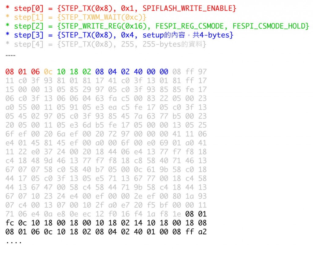
基本上這邊東西比較簡單,就是把我們剛剛準備好的那堆"step[]"轉成一個一維的陣列,
變成類似下面這個東西:
Debug: 30254 14838 fespi.c:692 as_compile(): 5511-byte program:
Debug: 30255 14838 fespi.c:697 as_compile(): 08 01 06 0c 10 18 02 08 04 02 40 00 00 08 ff 97
Debug: 30256 14838 fespi.c:697 as_compile(): 11 c0 3f 93 81 01 81 17 41 c0 3f 13 01 81 ff 17
Debug: 30257 14838 fespi.c:697 as_compile(): 15 00 00 13 05 85 29 97 05 c0 3f 93 85 85 fe 17
Debug: 30258 14838 fespi.c:697 as_compile(): 06 c0 3f 13 06 06 04 63 fa c5 00 83 22 05 00 23
Debug: 30259 14838 fespi.c:697 as_compile(): a0 55 00 11 05 91 05 e3 ea c5 fe 17 05 c0 3f 13
Debug: 30260 14839 fespi.c:697 as_compile(): 05 45 02 97 05 c0 3f 93 85 45 7a 63 77 b5 00 23
Debug: 30261 14839 fespi.c:697 as_compile(): 20 05 00 11 05 e3 6d b5 fe 17 05 00 00 13 05 25
Debug: 30262 14839 fespi.c:697 as_compile(): 6f ef 00 20 6a ef 00 20 72 97 00 00 00 41 11 06
Debug: 30263 14839 fespi.c:697 as_compile(): e4 01 45 81 45 ef 00 a0 00 6f 00 e0 69 01 a0 41
Debug: 30264 14839 fespi.c:697 as_compile(): 11 22 e0 37 24 00 20 18 44 06 e4 13 77 f7 f8 18
Debug: 30265 14839 fespi.c:697 as_compile(): c4 18 48 9d 46 13 77 f7 f8 18 c8 58 40 71 46 13
Debug: 30266 14839 fespi.c:697 as_compile(): 67 07 07 58 c0 58 40 b7 05 00 0c 61 9b 58 c0 18
Debug: 30267 14839 fespi.c:697 as_compile(): 44 17 05 c0 3f 13 05 e5 71 13 67 77 00 18 c4 58
Debug: 30268 14839 fespi.c:697 as_compile(): 44 13 67 47 00 58 c4 58 44 71 9b 58 c4 18 44 13
Debug: 30269 14839 fespi.c:697 as_compile(): 67 07 10 23 24 e4 00 ef 00 00 2e ef 00 80 1a 93
Debug: 30270 14839 fespi.c:697 as_compile(): 07 c4 00 13 07 00 10 2f a0 e7 20 f5 bf 00 00 11
Debug: 30271 14839 fespi.c:697 as_compile(): 71 06 e4 0a e8 0e ec 12 f0 16 f4 1a f8 1e 08 01
Debug: 30272 14839 fespi.c:697 as_compile(): fc 0c 10 18 00 18 00 10 18 02 14 10 18 00 18 08
Debug: 30273 14839 fespi.c:697 as_compile(): 08 01 06 0c 10 18 02 08 04 02 40 01 00 08 ff a2
Debug: 30274 14839 fespi.c:697 as_compile(): e0 a6 e4 aa e8 ae ec b2 f0 b6 f4 ba f8 be fc 42
Debug: 30275 14839 fespi.c:697 as_compile(): e1 46 e5 4a e9 4e ed 52 f1 56 f5 5a f9 5e fd e2
Debug: 30276 14839 fespi.c:697 as_compile(): e1 e6 e5 ea e9 ee ed f2 f1 f6 f5 fa f9 fe fd 73
Debug: 30277 14839 fespi.c:697 as_compile(): 25 20 34 f3 25 10 34 0a 86 ef 00 e0 3b 73 10 15
Debug: 30278 14839 fespi.c:697 as_compile(): 34 b7 22 00 00 9b 82 02 80 73 a0 02 30 a2 60 42
Debug: 30279 14839 fespi.c:697 as_compile(): 61 e2 61 02 72 a2 72 42 73 e2 73 06 64 a6 64 46
Debug: 30280 14839 fespi.c:697 as_compile(): 65 e6 65 06 76 a6 76 46 77 e6 77 0a 68 aa 68 4a
Debug: 30281 14839 fespi.c:697 as_compile(): 69 ea 69 0a 7a aa 7a 4a 7b ea 7b 0e 6c ae 6c 4e
Debug: 30282 14839 fespi.c:697 as_compile(): 6d ee 6d 0e 7e ae 7e 4e 7f ee 7f 11 61 73 00 20
Debug: 30283 14839 fespi.c:697 as_compile(): 30 01 a0 00 00 00 00 67 80 00 00 b7 27 00 20 d8

.......後面很多
這個一維的陣列就是我們小程式,所需要執行的程式碼XDD,
可以參考下圖:
最後是5,寫入準備好的"程式碼":
        int retval = target_write_buffer(target, data_wa->address, bytes,
                data_buf);
        if (retval != ERROR_OK) {
            LOG_ERROR("Failed to write data to 0x%" TARGET_PRIxADDR ": %d",
                    data_wa->address, retval);
            return retval;
        }
然後是6,執行小程式,並等待結果:
        retval = target_run_algorithm(target, 0, NULL, 2, reg_params,
                algorithm_wa->address, algorithm_wa->address + 4,
                10000, NULL);
        if (retval != ERROR_OK) {
            LOG_ERROR("Failed to execute algorithm at 0x%" TARGET_PRIxADDR ": %d",
                    algorithm_wa->address, retval);
            return retval;
        }
注意這邊,程式最後應該會停在小程式"0x4 ebreak"的位置,等待OpenOCD做進一步的處理!
怎麼樣啊!! 是不是很有趣啊!!! 再次把程式碼塞好塞滿
不過要特別提醒一下,不同廠牌的SPI NOR Flash有可能會有不同的Command,
在使用上的時候,務必小心!
根據測試的結果,約莫有10x ~ 30x速度的進步!
當然使用這套方法的前提是Target端必須要有一個可以跑小小程式的地方(可讀可寫可執行)!
在鐵人賽最後的兩篇中,我們將探討更上層的GDB,看看GDB和OpenOCD之前的關係,
以及簡單的介紹GDB Remote Protocol!
这段spi flash 的code 在被烧录到flash 之前,是存放在 riscv 芯片内部的哪个地址空间? (0x8000_0000, 0x9000_0000, 0x4000_0000 ?) 如何选择地址空间呢?
这段是spi flash 的烧写 程序, 它被存放在riscv 芯片中的哪个地址空间呢? (0x8000_0000, 0x9000_0000, 0x4000_0000 ?) 如何选择地址空间呢?
0x8000_0000
由OpenOCD的config決定的,可以參考這一行
$_TARGETNAME configure -work-area-phys 0x80000000 -work-area-size 10000 -work-area-backup 1
對應E51的DTIM區
你好, 首先感谢你的回答。
目前,我正在设计一个自己的risc-v的cpu, 基本的功能都是可以跑通的, jtag 也可以正常工作。目前想使用jtag 下载软件 程序到spi flash中去。 spi flash 的controller 也是写好了,能够正常的工作(我自己写的软件driver 可以正常的读写spi flash)使用的也是sifive 公司的 spi controller 架构(register 地址 和sifive 定义的相同)。
当我编写一段软件 app (比如 hello world) 可以使用
$_TARGETNAME configure -work-area-phys 0x80000000 -work-area-size 10000 -work-area-backup 1
正常的下载到芯片内部的程序存储空间(dtim)中, 并且通过jtag 接口看到相应的 assemble code. 地址确实是0x8000_0000 开始的,运行也没有问题。
我目前的问题是:
1)
.global _start
_start:
command_table:
j main // 0
ebreak // 4
j tx // 8
j txwm_wait // 12
j write_reg // 16
j wip_wait // 20
j set_dir // 24
// Execute the program.
main:
lbu t0, 0(a1)
addi a1, a1, 1
la t1, command_table
add t0, t0, t1
jr t0
这段代码被存放在dtim 的什么位置了, 怎么没有找到? (是否需要在软件中的lds 文件 或者是 startup.s 文件中需要相关的设置 才可以导入这段代码到 dtim 中 ?
2) -work-area-size 10000 是存放问题1 中的代码吗? 地址是 0x8000_0000 -- 0x8000_0000 + 10000 这个位置吗。
3) 最后软件生成的hello.elf (举例) 存放在什么位置呢? 是芯片内部的data memory 中吗, 地址又是怎么确定的呢。 在jtag 的cfg 文件中,没有找到相关的设定。
谢谢了
(1)(2)这段代码被存放在dtim 的什么位置了, 怎么没有找到?
這段代碼會放在"$TARGETNAME configure -work-area-phys 0x80000000 -work-area-size 10000 -work-area-backup 1"中指定的位置,也就是0x80000000 -- 0x8000000 + 10000這個區間沒錯,不過只有在需要時(也就是burn flash)才會被加載到那個區間中,當使用完畢後,OpenOCD會將原本區間中的資料還原回去!
(3) Elf(也就是你的程序)其存放位置由lds文件決定,至於放置的位置,有些是整個加載到DRAM,有些是將指令加載到ILM,另外將資料(變數...等等)放到DLM中,端看設計/需求而定
你好,感谢你的回答。
问题1,2 我听明白了, (需要实践一下, 看看是否工作)
问题3 可能是我没有说清楚.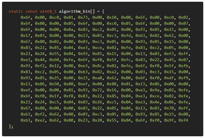
上图中所说的code (这个code ,我想应该是包括 elf 的 所有内容, 同时又增加了写入flash 的格式) 存放在什么位置呢?需要修改lds 文件吗?
下面code 是我目前的lds 文件:
OUTPUT_FORMAT( "elf32-littleriscv" )
OUTPUT_ARCH( "riscv" )
OUTPUT( "asm_temp.bin" )
/* STARTUP( "startup.o" ) */
ENTRY(_start)
_STACK_SIZE = 0x800;
_HEAP_SIZE = 0x1000;
MEMORY
{
rom (rx) : ORIGIN = 0x80000000, LENGTH = 32K
ram (wx!r) : ORIGIN = 0x90000000, LENGTH = 16K
}
SECTIONS
{
/* ================================= . = 0x80000000; ===================================== /
.init :
{
KEEP ((SORT_NONE(.init)))
} >rom AT>rom
.text  :
{
    *(.text .text.*)
} >rom AT>rom

.rodata :
{
    *(.srodata .srodata.*)
    *(.rodata .rodata.*)
    *(.rdata .rdata.*)
} >rom AT>rom

/* save at rom , will be use to load to 0x9000_00000 .data .sdata etc*/
.lalign         :
{
. = ALIGN(8);
PROVIDE( _data_lma = . );
} >rom AT>rom
/* ================================= . = 0x90000000; ===================================== */
/* start address of .data .sdata ,  data come from rom address */
.dalign         :
{
	. = ALIGN(8);
PROVIDE( _data_start = . );
} >ram AT>rom

.data :
{
    *(.sdata .sdata.*)

    . = ALIGN(8);
    *(.data .data.*)
} >ram AT>rom

. = ALIGN(8);
PROVIDE( _data_end = . );

.bss :
{
. = ALIGN(8);
    PROVIDE( __bss_start = . );
    *(.sbss*)
    *(.bss .bss.*)
    *(COMMON)
    . = ALIGN(4);

. = ALIGN(8);
    __bss_end = .;
    PROVIDE( __bss_end = . );
} >ram AT>ram

. = ALIGN(8);
PROVIDE( _end = . );
PROVIDE( end = . );

.heap ORIGIN(ram) + LENGTH(ram) - _STACK_SIZE - _HEAP_SIZE :
{
    _heap_begin = .;
    __heap_start = .;
    PROVIDE( __heap_start = . );
    . = . + _HEAP_SIZE;
    . = ALIGN(16);
    __heap_end = .;
    PROVIDE( __heap_end = . );

} >ram AT>ram


.stack ORIGIN(ram) + LENGTH(ram) - _STACK_SIZE :
{
    . = _STACK_SIZE;
    PROVIDE( _sp = . );
} >ram AT>ram
}
上图中所说的code (这个code ,我想应该是包括 elf 的 所有内容, 同时又增加了写入flash 的格式) 存放在什么位置呢?
algorithm_bin會在需要時被加載到0x80000000中
需要修改lds 文件吗?
不需要

