iT邦幫忙

第 12 屆 iThome 鐵人賽

DAY 7
1
IoT

熟悉Arduino的Maker必看!30天帶你快速入門基於STM32嵌入式開發~系列 第 7

[Day 7]-【STM32系列】淺入淺出之 General Purpose Input/Output 介紹 (上)

  • 分享至 

  • xImage
  •  

在STM32 CPU的架構裡面,CPU在和其他像是記憶體、DMA...等等的溝通時
資料會經由匯流排傳輸,匯流排就好像一台公交車,大家都得透過公車到達目的地

https://ithelp.ithome.com.tw/upload/images/20201019/20120093RJOjcWg6xw.png
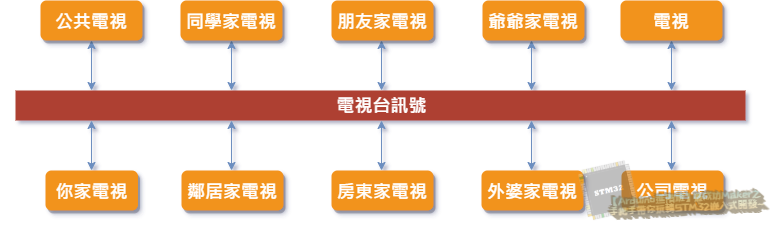
這很像甚麼?你知道大家的電視是怎麼連到第四台的嗎,概念類似電視台那邊釋出一條大的傳輸線

所有人你爸你媽你兄弟姊妹、子女、公公婆婆、岳父岳母、外公外婆、爺爺奶奶、五叔六嫂,四舅二伯、姑姑三姨、姊夫妹婿、外曾祖父母全部~全部的電視都連到電視台,第四台訊號就是匯流排,上面搭載著電視訊號。

下面一個CPU Bus架構的示意圖
https://ithelp.ithome.com.tw/upload/images/20200922/20120093wiThukt7ch.png

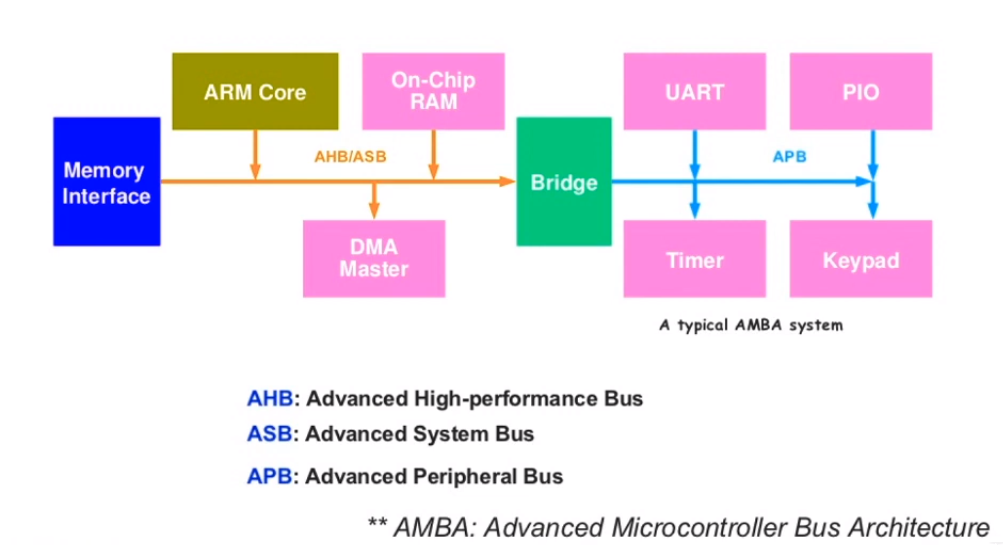
如上圖,CPU(ARM Core)連著AHB(Advanced High-performance Bus) 再和其他RAM、DMA設備等等的這些高速的東西相連,再連到外面的那些周邊的裝置則是APB (Advanced Peripheral Bus)

這兩者有甚麼不同呢?
AHB(Advanced High-performance Bus)主要連接速度非常快、高性能的裝置
APB (Advanced Peripheral Bus)連接GPIO、TIMER這些外部的周邊裝置
CPU及CPU附近的裝置的速度非常非常快
但是周邊的速度遠遠不及CPU這類的速度啊!實在是太慢了!
所以AHB再通過Bridge提供一個慢速的IO裝置

今天準備介紹的GPIO就是屬於周邊的IO裝置,當CPU要跟IO做控制時會經過APB (Advanced Peripheral Bus)連到中間Bridge這個控制器,負責跟CPU溝通最後才到CPU手中。

General Purpose Input/Output (GPIO)-簡介

GPIO(General Purpose Input/Output)是一種泛用型的輸入輸出裝置
可以當LED輸出,像上上篇範例的功能,也可以當按鈕的輸入
馬達控制,控制連續的High、Low變化產生PWM
當USB、USART...等等通訊協定的變化

可以想像是開關,user透過軟體可以自由打開關閉
每個GPIO可以是 input、output、analog或其他功能取決於要如何使用
所以總結來說它是一個通用型的,泛用型的輸入、輸出裝置。

下面是一個內部的結構方塊圖,我們主要看 GPIO PORT的部分
https://ithelp.ithome.com.tw/upload/images/20200928/20120093CrRMfxAWLF.png
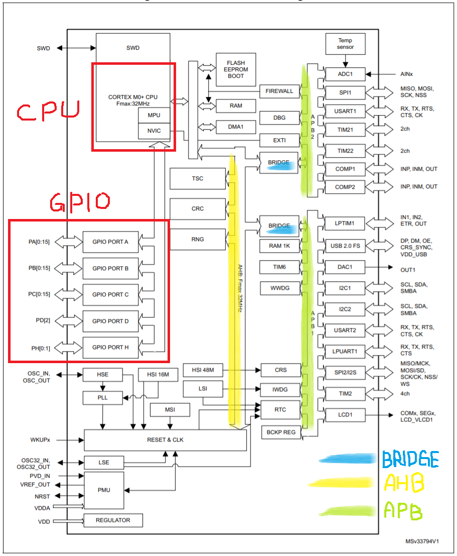
玩過8051的朋友應該知道GPIO就類似於8051的P0~P3
每一組IO都是8位元的暫存器,P0、P1、P2及 P3。

那在STM32L053R8這顆MCU裡面擁有五組GPIO的PORT
GPIOA、GPIOB、GPIOC、GPIOD和 GPIOH。而每一個PORT有16個bit
但並不是每個腳都是拿來做GPIO用,有些是拿來共用其他的功能,也有些是沒有拉出來的
那主要這塊板子能夠對外做GPIO跟外界溝通的只有GPIOA、GPIOB和GPIOC而已

還記得第二天提到過,現在使用的這塊開發版的腳位相容於Arduino的腳位
但這塊板子太強大了,若是只有使用Arduino的腳位就太浪費了
所以額外又多了更多的腳位
大家可以重新看到下面腳位的資訊

相容於原生Arduino腳位-左排

https://ithelp.ithome.com.tw/upload/images/20200922/201200930p8dJGhRYf.png

相容於原生Arduino腳位-右排

https://ithelp.ithome.com.tw/upload/images/20200922/2012009389vgwmwiOI.png

完整開發版腳位-左排

https://ithelp.ithome.com.tw/upload/images/20200922/20120093suWDAOdpKu.png

完整開發版腳位-右排

https://ithelp.ithome.com.tw/upload/images/20200922/20120093JX8G4GsHjl.png

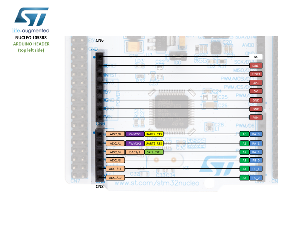
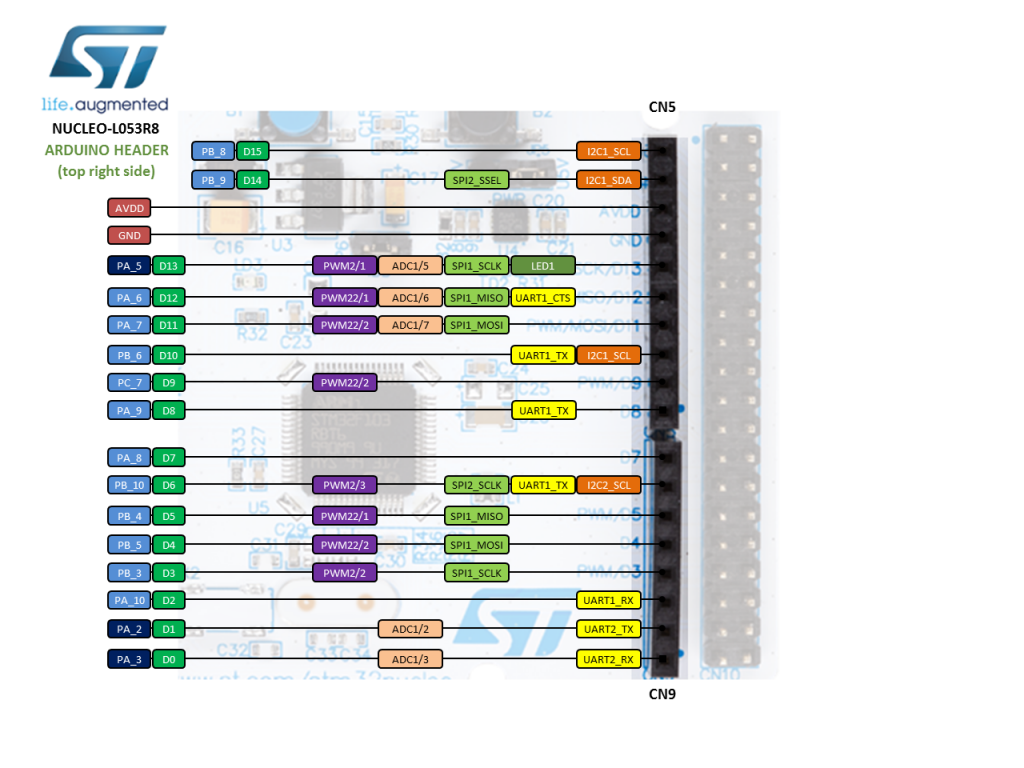
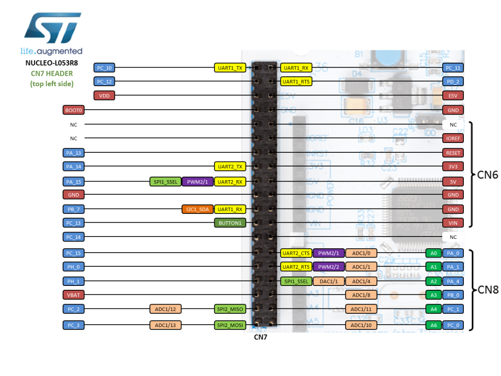
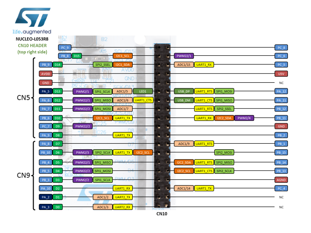
最常用的就是那些PB3、4、5或是PA5、6、7把這些IO拉出來做控制,達到我們要的效果
其實在這邊我們就可以看到不管是相容於原生Arduino的腳位還是完整開發版的腳位
每一個IO可能有不只一種功能,那既然一個引腳可以用於輸入、輸出或其他特殊功能
那麼一定有暫存器用來選擇這些功能,這部分後面會談到

STM32L053R8 GPIO特性

  • 所以每個GPIO引腳都可以透過軟體配置輸入輸出是否提供上拉電阻,是設置為開漏(open-drain,漏極開路)或推輓(push-pull)
  • 每個GPIO輸出的速度提供四種選擇(40 MHz,10 MHz,2 MHz,400 kHz)
  • 最大 I/O 切換速度可以支援到 32 MHz
  • 每個 GPIO Port 有 10 個 32-bit 暫存器 (Register)
    • GPIOx_MODER, GPIOx_OTYPER, GPIOx_OSPEEDR 與 GPIOx_PUPDR
    • GPIOx_IDR and GPIOx_ODR
    • GPIOx_BSRR and GPIOx_BRR
    • GPIOx_LCKR
    • GPIOx_AFRH 與 GPIOx_AFRL

GPIO腳位功能大致上可被設定為input(輸入)、output(輸出)、alternate function(特殊功能,比如pwm,timer,USART等等功能)或analog(類比)

通常在設置output的時候常會見到兩種模式:開漏(open-drain,漏極開路)和推輓(push-pull),這兩種模式差在哪裡呢?

1.Push-Pull推輓輸出

https://ithelp.ithome.com.tw/upload/images/20200922/20120093jkfMJ3sZcj.png
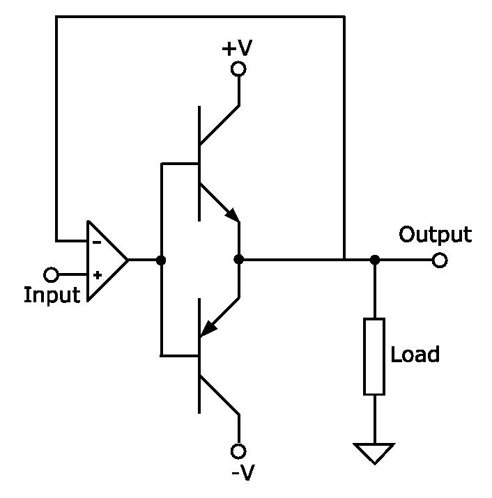
間單來說Push-Pull內部有一個P-MOS和一個N-MOS兩個互補的MOSFET組成,當上面的電晶體導通,下面的電晶體關閉輸出高電位;反之,上面的電晶體截止,下面的電晶體導通,輸出低電位。所以這個Push-Pull的電壓是由自己提供,所以電壓轉換速度快,可以吸電流,也可以貫電流是他的優點。除非有需要高阻抗狀態,否則一般不需要額外的上拉電阻。

2.Open-Drain開漏輸出

https://ithelp.ithome.com.tw/upload/images/20200922/201200938tc9DwE1hC.png
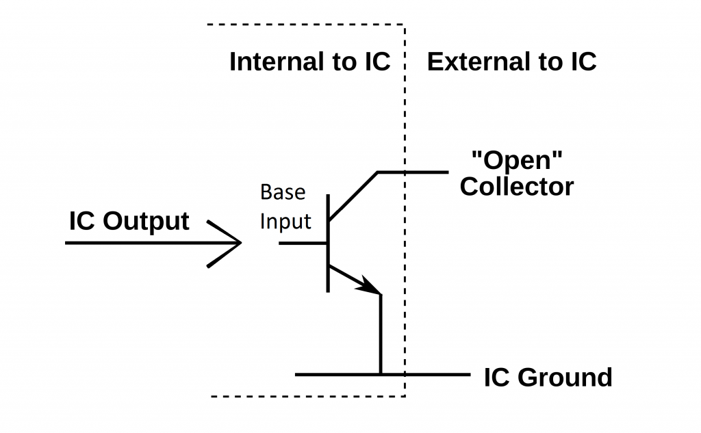
Open-Drain就是比Push-Pull少了上面那個電晶體,所以當下面的電晶體關閉,就輸出高電壓,但輸出是開路的,所以要加上拉電阻,則輸出的電壓就是由外界所提供,好處是外部電壓可以自己決定,改變上拉電阻的電壓,就可以調整邏輯High的準位。

Open-Drain 與Push-Pull的電路比較:

名稱 | 電路 | 特點
------------- | -------------
Open-Drain開漏輸出 | https://ithelp.ithome.com.tw/upload/images/20200922/20120093jkfMJ3sZcj.png | 1.可做電壓轉換-Level shift 2.Vo由外界提供,IC內部僅需很小的閘極驅動電流 3.可改變上拉電阻的電壓,調整邏輯High的準位。
Push-Pull推輓輸出 | https://ithelp.ithome.com.tw/upload/images/20200922/201200938tc9DwE1hC.png | 1.可以吸電流。2.可以灌電流。3.輸出電壓由IC電源決定。


GPIO Mode configuration

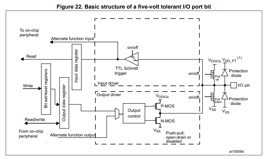
可以稍微看過GPIO在不同模式下的原理圖,這些資料可以在RM0367 Reference manual找到

1. Input configuration (P.242, 9.3.9 Input configuration in Reference manual)

https://ithelp.ithome.com.tw/upload/images/20200922/201200932PR7WLQqMS.png
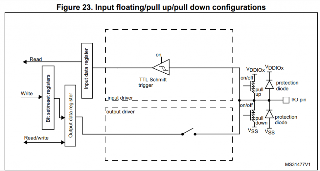
When the I/O port is programmed as input:

  • The output buffer is disabled
  • The Schmitt trigger input is activated
  • The pull-up and pull-down resistors are activated depending on the value in the GPIOx_PUPDR register
  • The data present on the I/O pin are sampled into the input data register every AHB clock cycle
  • A read access to the input data register provides the I/O state

2. Output configuration (P.242, 9.3.10 Output configuration in Reference manual)

https://ithelp.ithome.com.tw/upload/images/20200922/20120093JLyJBoAZkA.png
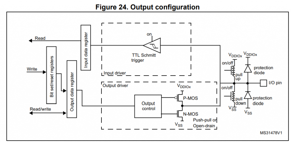
When the I/O port is programmed as output:

  • The output buffer is enabled:
    – Open drain mode: A “0” in the Output register activates the N-MOS whereas a “1” in the Output register leaves the port in Hi-Z (the P-MOS is never activated)
    – Push-pull mode: A “0” in the Output register activates the N-MOS whereas a “1” in the Output register activates the P-MOS
  • The Schmitt trigger input is activated
  • The pull-up and pull-down resistors are activated depending on the value in the GPIOx_PUPDR register
  • The data present on the I/O pin are sampled into the input data register every AHB clock cycle
  • A read access to the input data register gets the I/O state
  • A read access to the output data register gets the last written value

3. Alternate function configuration (P.244, 9.3.11 Alternate function configuration in Reference manual)

https://ithelp.ithome.com.tw/upload/images/20200922/20120093WySxdludcl.png
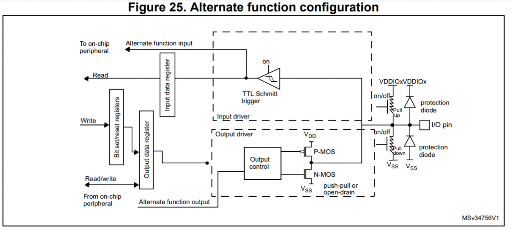
When the I/O port is programmed as alternate function:

  • The output buffer can be configured in open-drain or push-pull mode
  • The output buffer is driven by the signals coming from the peripheral (transmitter enable and data)
  • The Schmitt trigger input is activated
  • The weak pull-up and pull-down resistors are activated or not depending on the value in the GPIOx_PUPDR register
  • The data present on the I/O pin are sampled into the input data register every AHB clock cycle
  • A read access to the input data register gets the I/O state

Note: The alternate function configuration described above is not applied when the selected alternate function is a LCD function. In this case, the I/O, programmed as an alternate function output, is configured as described in the analog configuration.


4.Analog configuration (P.244, 9.3.12 Analog configuration in Reference manual)

https://ithelp.ithome.com.tw/upload/images/20200922/20120093lQczf4gGAK.png
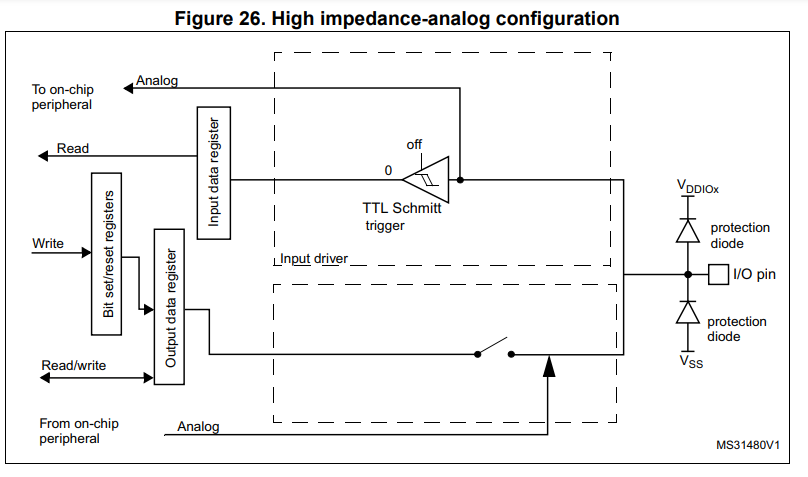
When the I/O port is programmed as analog configuration:

  • The output buffer is disabled
  • The Schmitt trigger input is deactivated, providing zero consumption for every analog value of the I/O pin. The output of the Schmitt trigger is forced to a constant value (0).
  • The weak pull-up and pull-down resistors are disabled by hardware
  • Read access to the input data register gets the value “0”

basic structure (P.237, Figure 22. Basic structure of a five-volt tolerant I/O port bit in Reference manual)

https://ithelp.ithome.com.tw/upload/images/20200922/20120093N5iAxtTwAf.png
在STM32CubeMX設定引腳時,產生的程式碼中就已經幫我們配置好設定的GPIO的MODER、OTYPER、OSPEEDR、PUPDR這些暫存器。
這邊介紹幾個之後會常用到的GPIO暫存器
8051中要設定P0~P3的數值只需要把1組8位元的值丟給P0~P3,實際上就是在間接控制暫存器
GPIOx的每一組暫存器都是32位元,只需把數值丟到指定的暫存器即可

  • IDR(input data register):input模式下GPIOx的讀值
  • ODR(output data register):output模式GPIOx的data
  • BSRR(port bit set/reset register):可單獨控制GPIOx其中1位元為High或Low,前16位元是set,後16位元reset
  • BRR(bit reset register):可單獨控制GPIOx其中一位元為LOW,只有前16位元可reset

MODE, TYPE, PuPd , SPEED 對應表

https://ithelp.ithome.com.tw/upload/images/20200922/20120093vgGLQJCFyh.jpg
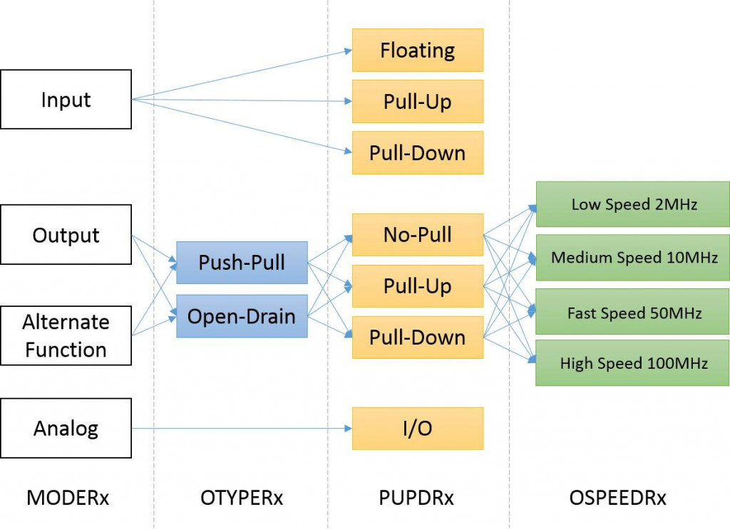
所以,以GPIO的某個引腳設定為任一MODER,以及設定甚麼TYPER,決定用內部推還是外部推,LED通常用內部推足夠了,然後決定上拉還是下拉來設定,最後是決定速度多快。

今天就到這裡
明天就要來玩模組啦


相關連結


結語

嗯...


上一篇
[Day 6]-【STM32系列】IoT開發中常見感測器介紹!
下一篇
[Day 8]-【STM32系列】淺入淺出之 General Purpose Input/Output 介紹 (下)
系列文
熟悉Arduino的Maker必看!30天帶你快速入門基於STM32嵌入式開發~30
圖片
  直播研討會
圖片
{{ item.channelVendor }} {{ item.webinarstarted }} |
{{ formatDate(item.duration) }}
直播中

1 則留言

0
inkdye
iT邦新手 5 級 ‧ 2021-08-12 09:30:19

您好:
  感謝您所提供學習資料,只是在[Open-Drain 與Push-Pull的電路比較:]這段落表格中,電路部分的圖示和上面段落所說的不同,煩請確認下,謝謝

poqwc5k6 iT邦新手 5 級 ‧ 2022-10-05 00:17:56 檢舉

好像是說明Open-Drain的時候使用了open-collector的圖說明

我要留言

立即登入留言